Printed Circuit Boards (PCBs) are the foundation of all modern electronics. But how exactly are they made?
This article breaks down the step-by-step PCB manufacturing process, revealing what happens behind the scenes—from raw materials to a fully functional circuit board.
Whether you’re a procurement manager, an engineer, or a startup founder, understanding the manufacturing process can help you make smarter supplier decisions, improve product quality, and reduce time to market.
What Is PCB Manufacturing?
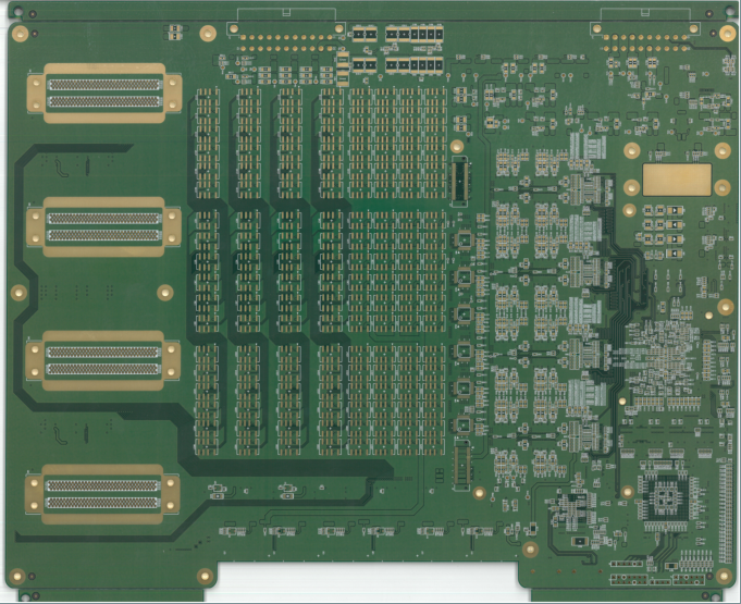
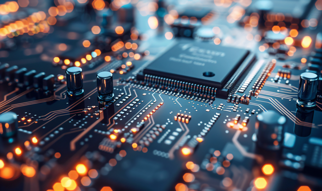
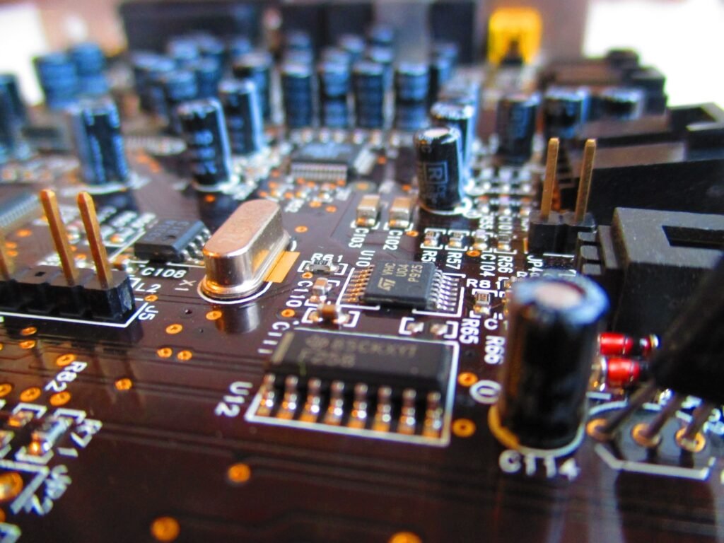
PCB manufacturing refers to the complex, multi-step process of turning a design file into a physical board using a mix of chemical, thermal, mechanical, and optical techniques. It includes inner and outer layer imaging, copper etching, lamination, drilling, plating, soldermask application, surface finish, and final testing.
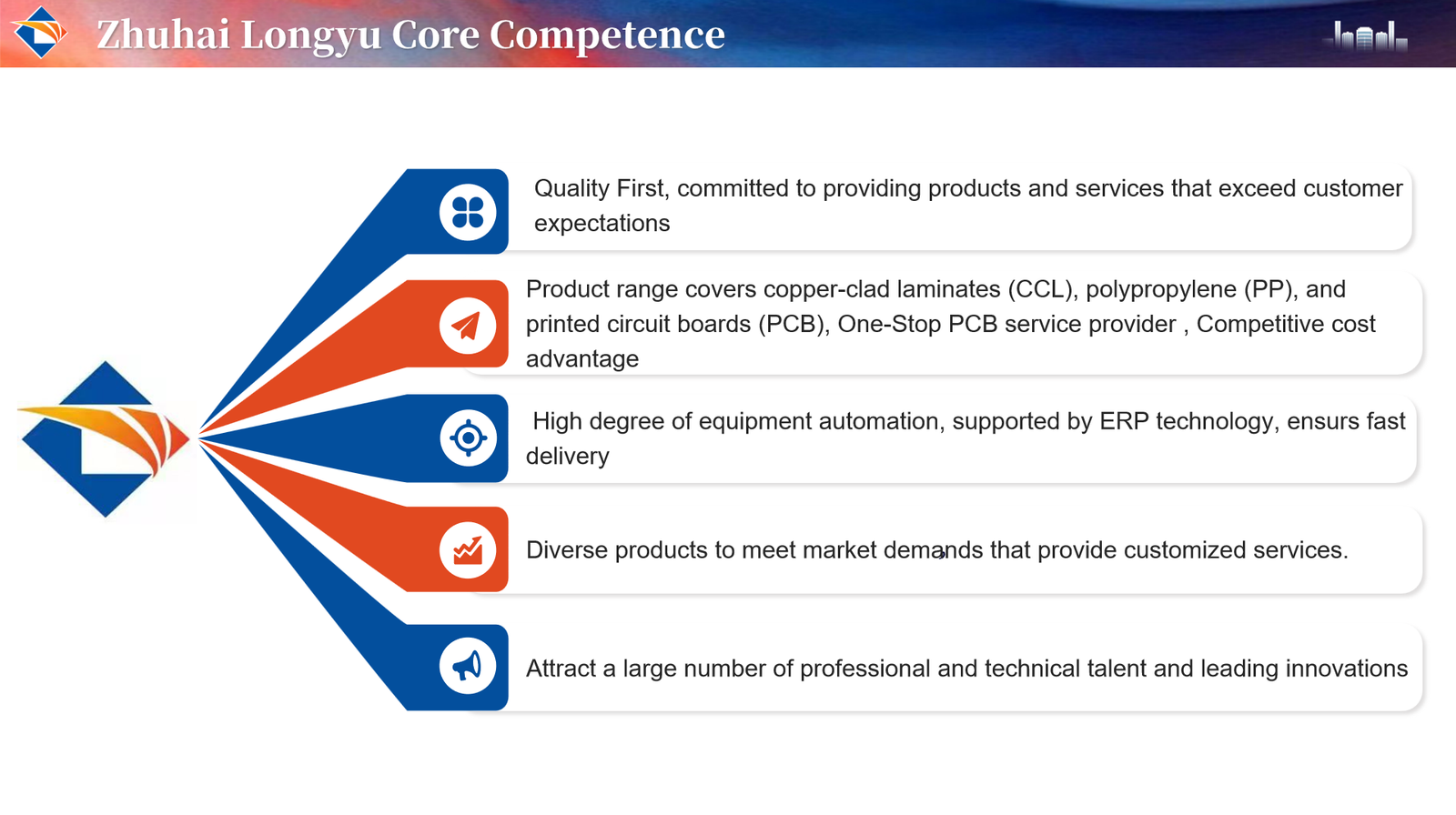
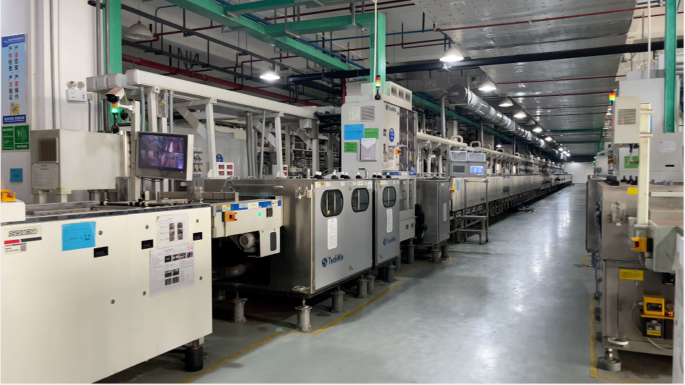
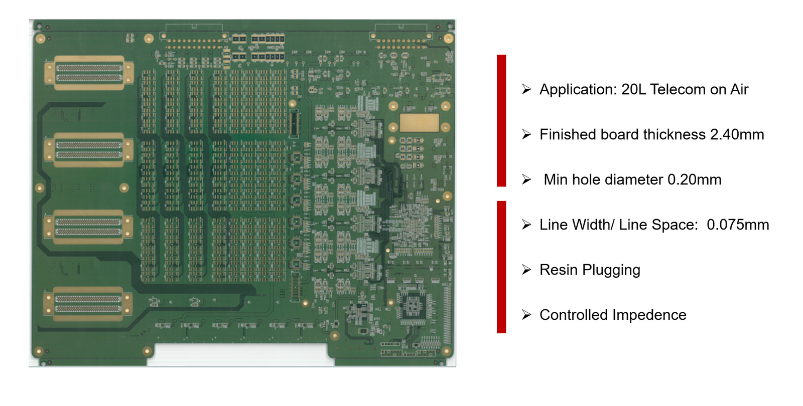
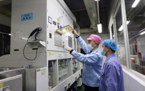
At Zhuhai Longyu, we operate advanced, fully automated production lines with monthly capacity of over 200,000㎡, certified by IATF16949, ISO9001, UL, ISO13485, and more.
Step-by-Step PCB Manufacturing Process
Step 1: PCB Design & CAM Data Preparation
Before production starts, Gerber files are submitted by the customer and verified by CAM engineers. These files define copper layers, drills, soldermask, silkscreen, and cut-outs.
| CAM Task | Description |
|---|---|
| Design Rule Check (DRC) | Verifies spacing, trace width, via size |
| Panelization | Arranges multiple boards for efficient production |
| Drill Map Alignment | Ensures hole sizes and locations match copper |
| Soldermask Optimization | Prevents mask from covering pads |

Step 2: Substrate Material Selection & Cutting
Boards typically use FR4, High-TG FR4, or Halogen-Free laminates, depending on heat tolerance and application.
| Material | Properties | Applications |
|---|---|---|
| FR4 | Standard Tg (~135°C), flame-retardant | Consumer electronics |
| High-TG FR4 | Tg >170°C | Automotive, high-speed |
| Halogen-Free | Eco-friendly, RoHS-compliant | Export to EU/US |
Step 3: Inner Layer Imaging and Etching
This is where the actual circuit paths are created. Dry film photoresist is applied to the copper-clad laminate. Circuit patterns are exposed using LDI (Laser Direct Imaging). Unexposed resist is removed, and copper is etched away.
Step 4: Multi-Layer Lamination
Layers are stacked with prepreg and laminated under heat and pressure.
| Lamination Stage | Details |
|---|---|
| Pre-alignment | Optical punching ensures layer registration |
| Pressing | 180–200°C and 2000 psi for 1–2 hours |
| Cooling | Controlled rate prevents warping or twist |
Note: Longyu uses 12-opening high-pressure lamination presses.
Step 5: Drilling (PTH, Blind/Buried Vias)
CNC drilling machines bore through the stack to form vias and through-holes.
| Hole Type | Description |
|---|---|
| PTH | Through-hole, copper-plated |
| Blind Via | Connects outer to inner layer only |
| Buried Via | Connects inner layers, not visible from outside |
| NPTH | Non-plated for mechanical use |
Step 6: Desmearing and Electroless Copper Plating
Drilled holes are chemically cleaned, and a thin layer (~1μm) of copper is deposited to ensure interlayer conductivity.
Step 7: Outer Layer Imaging and Pattern Plating
Photoresist is applied, and copper traces are plated before etching. This defines final outer circuitry.
Step 8: Soldermask Application
The green (or other colored) soldermask is applied and UV-cured.
| Feature | Spec |
|---|---|
| Thickness | ≥10μm |
| Color | Green, Blue, Black, White |
| Function | Insulation, solder bridge prevention |
Step 9: Surface Finish
Surface finishes protect copper and improve solderability.
| Finish Type | Typical Thickness | Application |
|---|---|---|
| ENIG | Ni: 3–6μm, Au: 0.05μm | BGA, fine pitch |
| HASL | 1–25μm | General electronics |
| OSP | <0.5μm | Short assembly cycles |
| Immersion Tin/Silver | Thin layer | RoHS-compliant export |
Step 10: Silkscreen Printing
Component identifiers, logos, and tracking info are printed using inkjet or screen printers.
Step 11: Profiling and V-Cutting
Boards are cut to final shape using CNC routers or V-cut machines.
| Process | Tolerance |
|---|---|
| Routing | ±0.1mm |
| V-Cut | ±0.2mm |
Step 12: Electrical Testing & Final Inspection
Every board is tested for electrical continuity and inspected visually.
| Test Type | Purpose |
|---|---|
| Flying Probe | Open/Short circuit detection |
| AOI/AVI | Defect detection & alignment |
| X-Ray | BGA & internal via inspection |
| Impedance Test | Signal integrity confirmation |
✔ IPC-A-600 Acceptability Standard
✔ UL PCB Manufacturer Certification
Why a Reliable PCB Manufacturing Process Matters
From design to delivery, every step in the PCB manufacturing process requires precision, consistency, and quality control. Even a minor error in imaging, drilling, or plating can lead to product failure.
Zhuhai Longyu combines automated production lines, strict IPC-compliant testing, and over 721 skilled workers across three industrial bases to ensure quality delivery.
- ✔ Certified Quality (IATF16949, UL, ISO9001)
- ✔ Mass Production Capacity (200,000㎡/month)
- ✔ 2–24 Layer PCB Solutions
- ✔ Automotive, LED, Telecom Expertise