In high-speed electronic design, the PCB stack-up—the arrangement of copper layers and dielectric materials—plays a pivotal role in ensuring signal integrity, power distribution, and electromagnetic compatibility (EMC).
A well-structured stack-up minimizes signal reflections, crosstalk, and EMI, while optimizing thermal performance and mechanical stability.
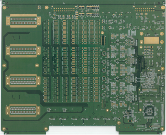
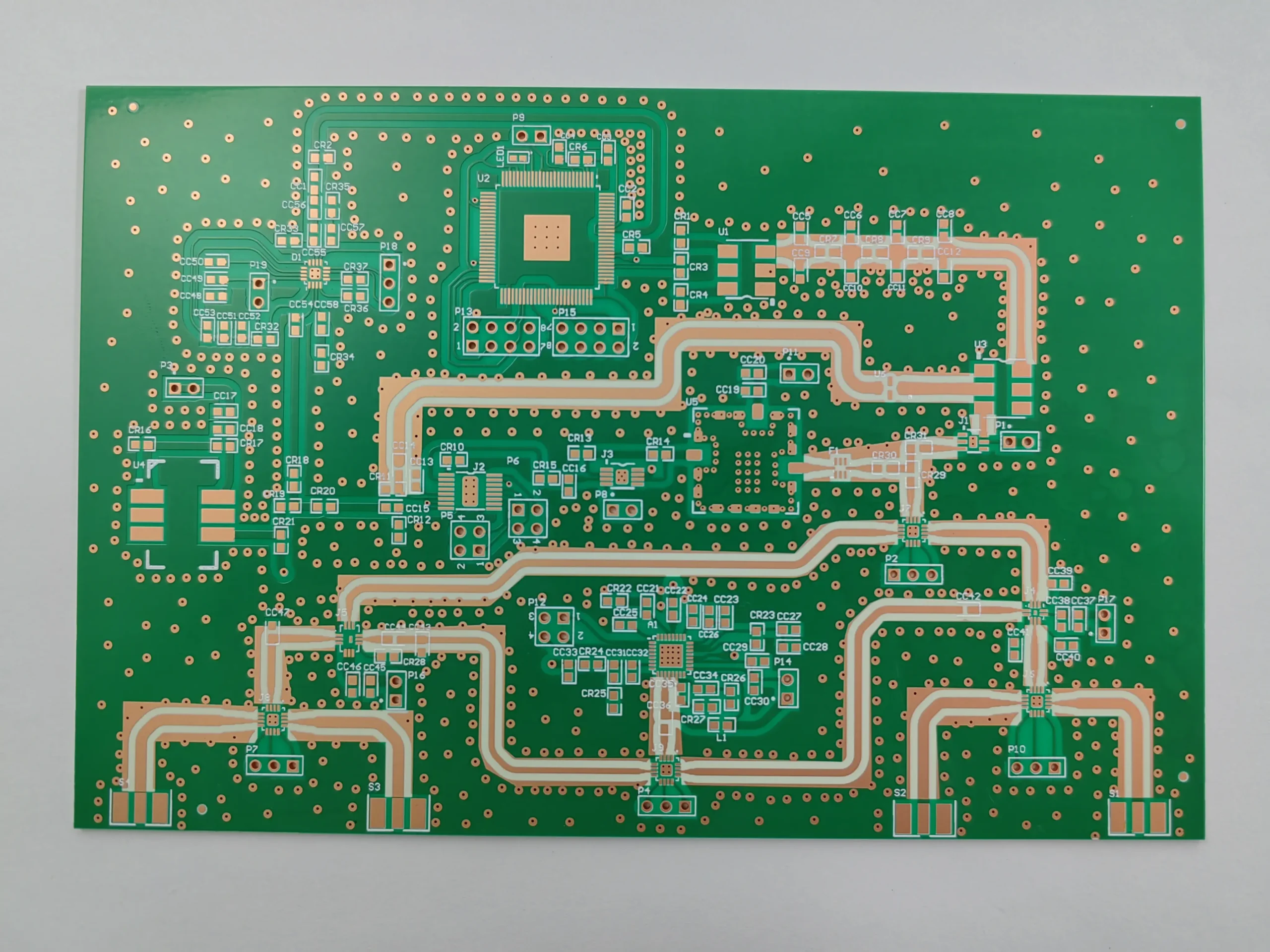
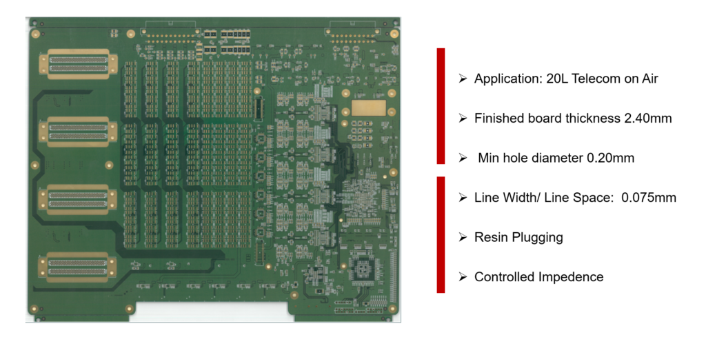
Longyu specializes in crafting multilayer PCBs with optimized stack-ups tailored for applications ranging from 5G telecommunications to medical devices.
This guide delves into the intricacies of PCB stack-up design, highlighting its significance and best practices.
What Is PCB Stack-Up?
A PCB Stack-Up refers to the vertical arrangement of copper layers and insulating materials (like FR4) in a multilayer PCB. It defines how signal and ground planes are positioned relative to each other and affects:
Signal Integrity: Proper stack-up minimizes crosstalk and electromagnetic interference.
Power Distribution: Stable power delivery across different layers.
Mechanical Stability: Supports structural integrity in compact and complex designs.
Why Is Stack-Up Important?
Before the development of multilayer PCBs, single-layer and double-layer boards dominated the market. As electronic devices became more compact and signal frequencies increased, designers faced challenges in signal integrity and power stability. The introduction of complex stack-up configurations addressed these challenges by:
Improving signal shielding through adjacent ground planes.
Reducing crosstalk with strategic layer placement.
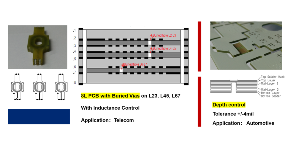
Supporting high-speed signal transmission with impedance-controlled stack-ups.
Key Takeaway: Optimizing stack-up design is essential for achieving reliable, high-speed data transmission in PCBs.

Common Types of PCB Stack-Up Structures
The choice of PCB stack-up structure depends on the design complexity, signal frequency, and application requirements. Here are some common types:
| Layer Count | Typical Structure | Applications |
|---|---|---|
| 2-Layer | Top Layer (Signal), Bottom Layer (Ground) | Simple consumer electronics |
| 4-Layer | Signal, Ground, Power, Signal | Industrial controls, audio systems |
| 6-Layer | Signal, Ground, Signal, Power, Ground, Signal | High-speed digital circuits, IoT devices |
| 8-Layer | Signal, Ground, Signal, Power, Power, Signal, Ground, Signal | Data servers, RF applications |
Design Tip: For high-speed designs, route signals between two ground planes to ensure a low-impedance return path and minimize EMI.
How PCB Stack-Up Affects Performance
1. Signal Integrity
Controlled impedance is crucial for high-frequency signal transmission. Impedance mismatches can cause reflections, leading to signal distortion. By carefully selecting dielectric materials and maintaining consistent trace geometries, designers can achieve the desired impedance levels.
2. Electromagnetic Compatibility (EMC)
EMC performance is enhanced by minimizing loop areas and ensuring proper shielding. Placing signal layers adjacent to ground planes and avoiding adjacent signal layers reduces crosstalk and radiated emissions.
3. Power Integrity
A solid power distribution network (PDN) is achieved by incorporating dedicated power and ground planes. This configuration reduces voltage fluctuations and ensures stable operation of high-speed components.
Choosing the Right PCB Stack-Up
1. Consider the Application Requirements
Low-Frequency Devices (≤1GHz): Two or four-layer boards usually suffice.
High-Frequency Devices (≥1GHz): Six-layer or more for signal integrity.
Compact Designs: Rigid-flex stack-up for space optimization.
2. Material Selection
FR4: Cost-effective, suitable for most general applications.
High-TG FR4: Required for high-heat environments.
Rogers: Best for RF and microwave circuits due to low dielectric loss.
3. Design Tips for Optimal Stack-Up
Maintain symmetry to avoid warpage.
Position ground planes close to signal layers.
Implement controlled impedance for high-speed signal traces.
Use thin dielectric layers to reduce inductance and capacitance.


Optimizing PCB Stack-Up for Performance and Reliability
Selecting the right PCB stack-up significantly impacts signal integrity, EMI resistance, and power management. As technology advances, designing a well-structured stack-up becomes essential for achieving optimal performance.
Whether you are developing IoT devices, industrial controls, or aerospace systems, consider your application requirements and consult with industry experts to ensure the best configuration.
Need expert guidance on PCB stack-up design? Contact Zhuhai Longyu Technology for expert advice on multilayer PCB stack-up solutions.
Frequently Asked Questions About PCB Stack-Up and Performance
Q1: Why is PCB stack-up important?
A: A well-designed stack-up ensures signal integrity, power stability, and EMC compliance, which are essential for reliable PCB performance.
Q2: How does stack-up affect impedance?
A: Impedance is influenced by trace width, dielectric constant, and the distance between signal traces and reference planes. Proper stack-up design maintains consistent impedance, reducing signal reflections.
Q3: Can I use the same stack-up for different applications?
A: While some stack-ups are versatile, it’s best to tailor the stack-up to specific application requirements, considering factors like signal frequency and power demands.