At Longyu PCB, we understand the critical role that vias play in multi-layer PCB design. As a professional PCB manufacturer, we provide advanced solutions for various applications, including automotive electronics, communication systems, and high-density interconnect (HDI) boards.
Vias enable reliable connections between different layers, maintaining signal integrity and managing heat dissipation.
In this guide, we will explore the types of vias, their functions, and best practices for using them effectively.
1. What Are Vias in Multi-Layer PCBs?
Vias are small holes drilled through PCB layers, filled with conductive material (usually copper), to create electrical connections between layers. They are essential for multi-layer PCBs, which contain complex circuits requiring reliable interlayer connections. Vias also help with thermal management by transferring heat from internal layers to the surface.
1.1 Why Vias Are Crucial in Multi-Layer PCBs
In multi-layer PCBs, vias connect internal signal, power, and ground layers. Without vias, routing signals efficiently across densely packed boards would be nearly impossible. They also aid in thermal dissipation, crucial in high-power applications. Improper via selection or placement can lead to signal degradation, increased resistance, or even mechanical failure.
For more technical standards, refer to the IPC-6012 Standard.
2. Types of Vias in Multi-Layer PCBs
2.1 Through-Hole Vias
Through-hole vias are drilled from the top layer to the bottom layer, passing through the entire PCB. They are filled or plated with copper to ensure continuity. Due to their simplicity, they are commonly used in low-cost, less complex boards.
- Pros: Cost-effective, simple to manufacture.
- Cons: Takes up space on every layer, not suitable for high-density designs.
- Applications: Industrial control systems, low-density PCBs.
- Example: At Longyu PCB, we use through-hole vias in durable industrial PCBs, ensuring reliable connections even under mechanical stress.
2.2 Blind Vias
Blind vias connect the outer layer to one or more inner layers without passing through the entire board. These vias are useful for saving space on dense boards where surface real estate is limited.
- Pros: Saves space, supports complex multi-layer structures.
- Cons: More expensive than through-hole vias, requires precision drilling.
- Applications: Automotive electronics, communication devices.
- Example: Our automotive PCBs often use blind vias to accommodate compact designs while maintaining electrical performance.
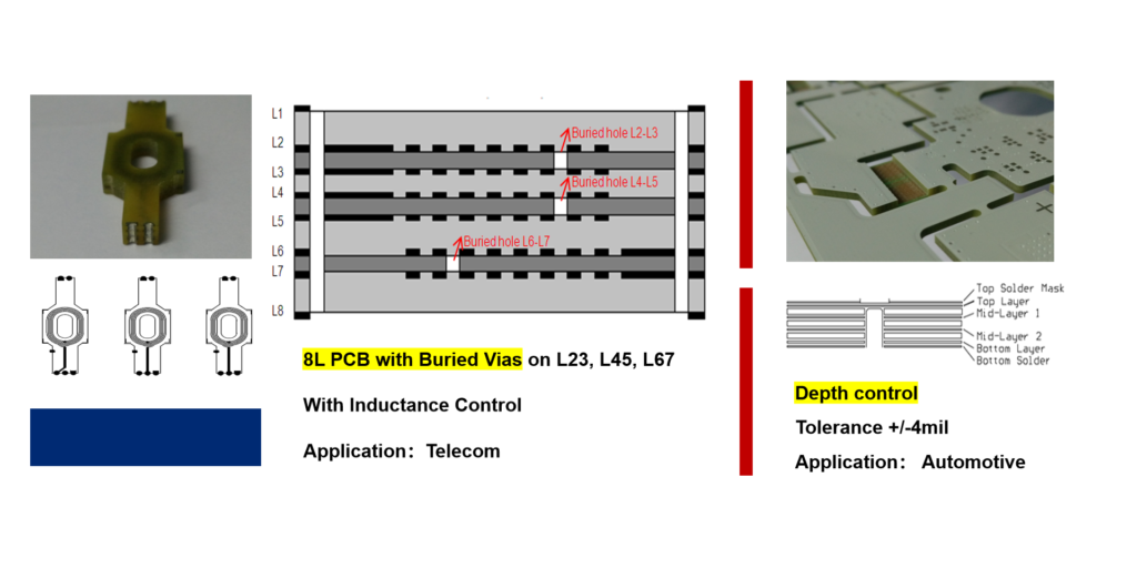
2.3 Buried Vias
Buried vias are entirely encapsulated within the internal layers of a PCB, making them ideal for high-density designs. They do not connect to the outer layers, conserving surface space.
- Pros: Efficient use of internal layers, no impact on outer layers.
- Cons: Complex manufacturing, higher cost.
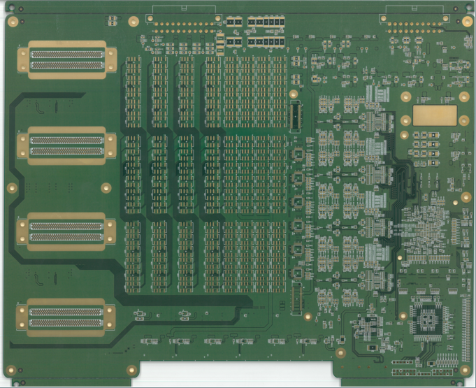
- Applications: High-frequency communication boards, multi-layer HDI PCBs.
- Example: Longyu PCB uses buried vias in HDI boards to optimize signal integrity and minimize layer interference.
2.4 Microvias
Microvias are small vias typically used in HDI PCBs. Their small size allows for higher interconnect density, suitable for modern compact devices.
- Pros: Supports compact, high-density designs, ideal for fine-pitch components.
- Cons: High cost, precision manufacturing required.
- Applications: Smartphones, tablets, compact communication devices.
- Example: At Longyu PCB, we use microvias in high-speed communication boards to ensure reliable signal transmission.
3. Best Practices for Via Design and Manufacturing
3.1 Optimize Via Placement
Proper via placement is crucial for signal integrity and thermal performance. Misplaced vias can introduce noise, reduce thermal efficiency, and cause signal loss.
At Longyu PCB, we carefully plan via locations using advanced design tools to minimize signal disruption and enhance durability.
- Signal Integrity: Offset vias from critical paths to reduce reflections.
- Thermal Management: Distribute thermal vias under heat sources for better heat dissipation.
- Mechanical Reliability: Reinforce vias with copper filling to withstand thermal cycling.
4. Real-World Applications: How Vias Enhance PCB Performance
Vias improve the performance of multi-layer PCBs in various applications:
- Automotive Electronics: Durable vias ensure stability under high temperatures.
- Communication Devices: Microvias maintain signal integrity in high-frequency applications.
- Industrial Control Systems: Through-hole vias enhance mechanical strength.
Optimizing Vias with Longyu PCB
Vias are essential for reliable multi-layer PCB functionality. Choosing the right type and optimizing its placement significantly improves signal integrity and thermal management.
Longyu offer advanced via solutions tailored to diverse applications, including automotive, communication, and high-density electronics.