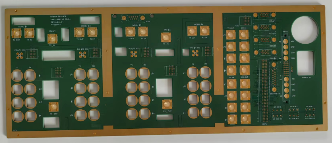
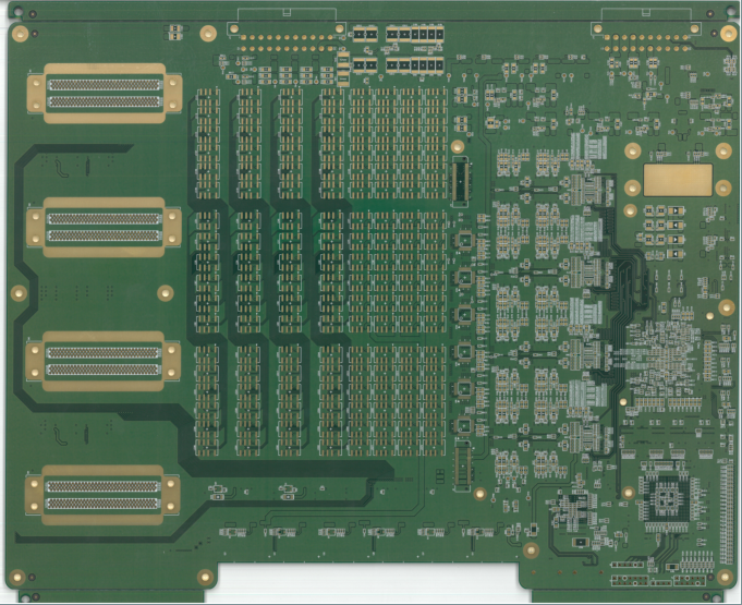
Designing a Printed Circuit Board (PCB) is a complex process that requires careful planning and meticulous attention to detail. Even small design flaws can lead to functional failures, signal integrity issues, and costly rework.
This article highlights the top 10 most common PCB design mistakes and provides practical tips on how to avoid them, helping engineers develop reliable and efficient PCBs.
1. Inadequate Trace Width Calculation
One of the most common mistakes in PCB design is failing to calculate trace width properly. An undersized trace can lead to excessive heat, voltage drops, and potential failures.
1.1 How to Avoid:
Use the IPC-2221 standard to calculate trace width based on current requirements. Online calculators such as 4PCB Trace Width Calculator can simplify the process.
| Current (A) | Trace Width (mil) | Recommended Standard |
|---|---|---|
| 1 | 10 | IPC-2221 |
| 2 | 20 | IPC-2221 |
| 3 | 30 | IPC-2221 |
2. Poor Component Placement
Improper placement of components can lead to signal integrity issues, increased EMI, and inefficient routing.
2.1 How to Avoid:
Follow a systematic approach by grouping components based on function and minimizing trace length. Use design software like Altium Designer for visual guidance.
3. Ignoring Grounding Techniques
Poor grounding can result in voltage fluctuations, signal noise, and electromagnetic interference (EMI).
3.1 How to Avoid:
Use a solid ground plane to reduce noise. Maintain consistent grounding paths and avoid ground loops. For more details, refer to IPC-2221 Grounding Guidelines.
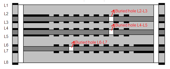
4. Incorrect Via Design
Vias are crucial for multi-layer PCB connectivity. Choosing incorrect via sizes or placing them improperly can cause signal loss and thermal issues.
4.1 How to Avoid:
Select via sizes based on current carrying capacity and signal frequency. Implement thermal relief for power vias to ensure heat dissipation.
5. Signal Integrity Problems
High-speed designs often suffer from signal integrity issues like crosstalk, reflection, and impedance mismatch.
5.1 How to Avoid:
Use controlled impedance traces and differential pair routing for high-speed signals. Maintain trace symmetry and adequate spacing.
6. Overcomplicated Routing
Complex routing increases signal delay and noise interference, especially in high-density boards.
6.1 How to Avoid:
Plan a clean and simple routing strategy, keeping trace lengths short and parallel signals separated. Use auto-routing features cautiously.
7. Insufficient Thermal Management
Failing to manage heat dissipation can lead to overheating and reduced lifespan of the PCB.
7.1 How to Avoid:
Use thermal vias, heat sinks, and copper pours to enhance heat dissipation. Refer to Thermal Dynamics Resources for advanced cooling techniques.
8. Missing Design Rule Checks (DRC)
Skipping DRC can result in rule violations, such as spacing errors and short circuits.
8.1 How to Avoid:
Always run DRC using CAD tools like KiCad or Eagle. Set up rules for spacing, trace width, and via sizes before finalizing the design.
9. Neglecting Power Integrity
Poor power distribution can cause voltage drops and insufficient current supply to critical components.
9.1 How to Avoid:
Implement a power plane for low-impedance paths and use decoupling capacitors to stabilize voltage. Follow the guidelines in Analog Devices Power Integrity Resources.
10. Lack of Testing Provisions
Designs without test points make debugging and quality assurance difficult.
10.1 How to Avoid:
Integrate test pads and boundary scan points during the design phase. Follow IEEE-1149.1 standards for effective testing.
Avoiding PCB Design Pitfalls: Key Takeaways
Avoiding common PCB design mistakes requires a combination of planning, adherence to industry standards, and the use of advanced design tools.
By recognizing and mitigating these errors, engineers can significantly reduce the risk of product failure and improve the reliability of their PCB designs.

Discover Reliable PCB Design with Longyu PCB
At Longyu PCB, we specialize in optimizing PCB designs to ensure quality and performance.