Printed Circuit Board (PCB) traces are crucial components that establish the electrical pathways between various elements on a circuit board.
These copper traces carry signals and power throughout the PCB, ensuring that the electronic device functions correctly. Optimizing PCB trace design is essential for maintaining signal integrity, minimizing interference, and ensuring product reliability.
In this article, we will explore the fundamentals of PCB traces, common design challenges, and practical optimization techniques.
1. Understanding PCB Traces: Types and Characteristics
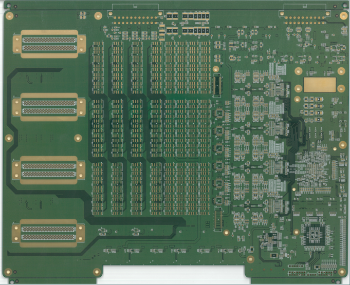
PCB traces are conductive pathways made of copper that form the wiring pattern on a PCB. The trace width, thickness, and length determine the current-carrying capacity and resistance. Understanding the different types of traces and their characteristics is essential for efficient PCB design.
1.1 Types of PCB Traces
- Signal Traces: Carry electrical signals between components.
- Power Traces: Provide power distribution to various components.
- Ground Traces: Connect to the ground plane, stabilizing voltage levels.
1.2 Key Trace Parameters
The critical parameters influencing trace performance include:
- Width: Affects current capacity and resistance.
- Thickness: Determines heat dissipation and current handling.
- Length: Influences resistance and voltage drop.
| Parameter | Impact | Optimization Tips |
|---|---|---|
| Width | Increases current capacity | Use wider traces for power lines |
| Thickness | Improves heat dissipation | Follow IPC-2221 standards |
| Length | Causes voltage drop | Minimize trace length for signal lines |
For more technical details, visit the IPC Official Website.

2. Challenges in PCB Trace Design
Designing PCB traces involves addressing multiple challenges related to signal integrity, thermal management, and space constraints. Inadequate trace design can lead to overheating, signal loss, and electromagnetic interference (EMI).
2.1 Signal Integrity Issues
Poor trace design can result in signal attenuation, crosstalk, and electromagnetic interference. High-frequency signals are particularly vulnerable to signal degradation due to trace impedance and inductance.
2.2 Thermal Management
Traces carrying high currents can overheat, leading to potential damage. Proper trace width and copper thickness are vital to handling the required current without excessive temperature rise.
2.3 Space Constraints
Compact PCBs with dense component layouts often limit trace width and spacing. Balancing trace width with available space while maintaining performance requires precise calculations.
3. Optimization Techniques for PCB Trace Design
Optimizing PCB traces ensures improved electrical performance, thermal stability, and signal integrity. Here are some best practices:
3.1 Calculating Trace Width
Use the IPC-2221 standard to calculate trace width based on current capacity:
Formula: W = (I / (k * ΔT^0.44))^1/b
- W: Width of the trace (in mils)
- I: Current (in amps)
- ΔT: Temperature rise (in °C)
- k, b: Constants from IPC-2221
Refer to the IPC-2221 Standard for more accurate calculations.
3.2 Minimizing Crosstalk
To reduce crosstalk, increase the spacing between parallel traces and use ground planes to shield signals. Differential pair routing can also enhance signal integrity in high-speed circuits.
3.3 Improving Thermal Management
Increasing trace width and thickness, especially for power traces, helps in dissipating heat effectively. Using multiple layers with ground and power planes also improves thermal conductivity.
 4. Simulation and Testing for Optimal Trace Performance
Advanced simulation tools, such as SPICE and HyperLynx, enable designers to model trace performance and detect potential issues before manufacturing.
4.1 Signal Simulation
Simulations help evaluate signal integrity and detect potential interference issues. Use tools like HyperLynx to model signal behavior under real-world conditions.
4.2 Thermal Analysis
Thermal simulation ensures that traces maintain safe temperatures during operation. Use simulation data to optimize trace dimensions and copper thickness.
5. Industry Standards and Compliance for PCB Traces
Adhering to industry standards such as IPC-2221 and IPC-6012 is essential for reliable PCB trace design.
5.1 IPC Standards
The IPC-2221 standard outlines general requirements for PCB design, including trace width, spacing, and copper thickness.
5.2 ISO Certification
ISO 9001 certification ensures that manufacturing processes meet quality management standards, reducing variability in PCB production.
Achieving Optimal PCB Trace Design for Reliable Performance
Properly designed PCB traces enhance electrical performance, reduce thermal stress, and minimize interference. By implementing industry best practices and adhering to standards, manufacturers can ensure long-lasting and reliable PCB products.