Modern electronics—from smartphones to satellites—would not function without Printed Circuit Boards (PCBs). As the silent infrastructure beneath every electronic device, PCBs form the backbone of electrical connectivity and mechanical support.
For engineers and B2B buyers alike, understanding how PCBs work, what types are available, and how to evaluate suppliers is essential for smarter sourcing and more reliable products.
What Is a PCB (Printed Circuit Board)?
A Printed Circuit Board (PCB) is a layered structure made of insulating materials (such as FR4) laminated with copper sheets.
These copper traces replace bulky wire connections and allow electrical signals to move between components in a compact, reliable way.
- Greater durability and signal integrity
- Repeatable manufacturing precision
Key PCB Components and Their Functions
- Substrate (FR4): The mechanical backbone. For high-temperature environments, use High-TG FR4 or ceramic materials.
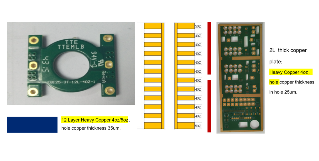
- Copper Layers: These are the ‘roads’ for current. Heavier copper is required in power electronics and industrial controls.
- Soldermask: Often green, but not always. It ensures solder goes where it should—especially critical in high-density boards.
- Silkscreen: Essential for post-assembly testing and rework.
- Vias:
- Through-hole → Standard communication between top and bottom layers
- Blind/Buried → Used in complex multilayer stack-ups
- Microvias → Essential for HDI designs like smartphones
Key takeaway: The choice of each layer affects cost, performance, and manufacturability.
Why PCBs Matter in Modern Electronics & Product Design
Increased Reliability
- Low signal loss
- Controlled impedance (vital for high-speed circuits)
- Repeatabl
Cost Optimization at Scale
- Lower labor requirements
- Standardized form factors
- Faster assembly line integration with SMT
Compliance & Safety
- Documented stack-ups
- Flame-retardant materials (UL94V-0)
- Controlled trace spacing and current capacity
Types of PCBs for Consumer, Automotive, and Industrial Use
Double-Layer PCBs
Double-layer: Ideal for consumer audio systems, small appliances.

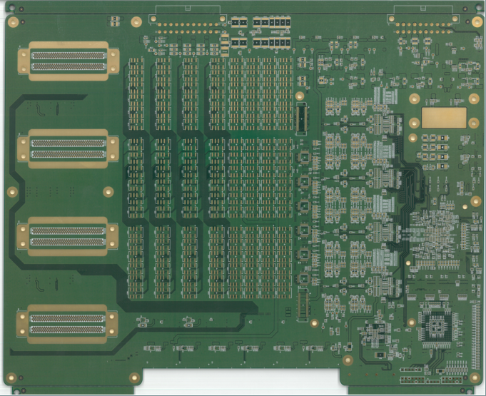
Multilayer PCBs
Used in high-speed and compact devices like smartphones, servers, and ECUs.
| Layer | Function |
|---|---|
| L1 | Signal |
| L2 | Ground Plane |
| L3 | Power Plane |
| L4 | Ground Plane |
| L5 | Signal |
| L6 | Signal |
PCB Manufacturing Process: Step-by-Step Overview
1. Design & Material Selection
- CAD software for layout and stack-up
- DFM feedback for compatibility
- Material choice based on application
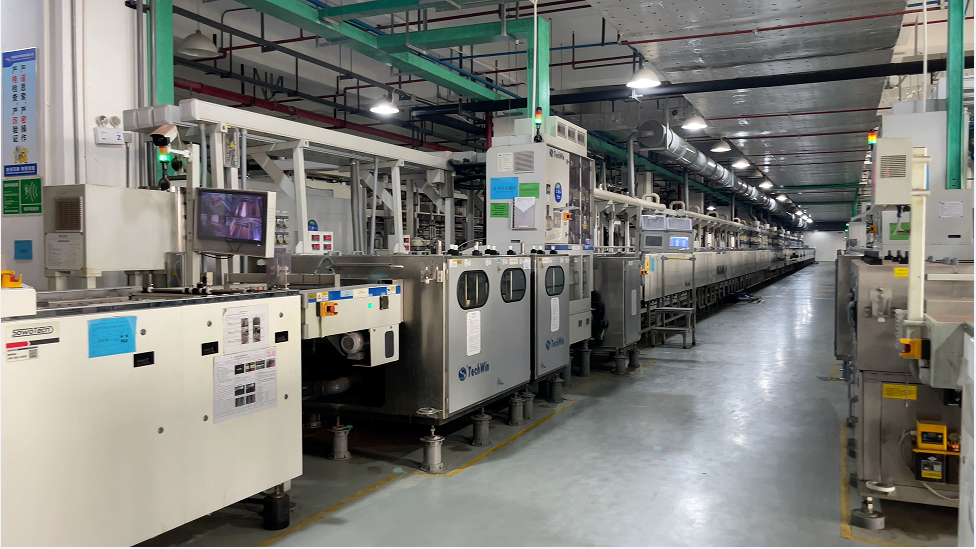
2. Fabrication Stages
- Lamination, drilling, etching
- Plating and coating (ENIG, HASL, OSP)
- Soldermask and silkscreen application
3. Testing & Inspection
- Electrical Testing (continuity/isolation)
- AOI, X-ray, and impedance testing
Understanding each step of the PCB manufacturing process—from design and lamination to drilling, etching, and final inspection—is essential for ensuring product reliability and manufacturability.
For a deeper dive into real-world fabrication techniques, material selection, and process control best practices, explore detailed PCB fabrication guides on PCBWay.
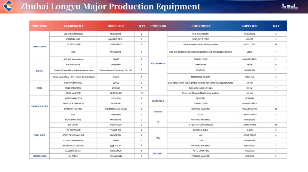
Zhuhai Longyu Technology provides full-process QC including flying probe testers, AOI, and certified systems.

How to Evaluate PCB Suppliers and Manufacturers
1. Certifications
- ISO9001, IATF16949, ISO13485, RoHS, UL
2. Capacity & Turnaround
- Volume capability (e.g., 200,000 m²/month)
- Prototyping + large-scale production
- Express shipping options
3. Engineering Support
- DFM reviews
- Stack-up and impedance simulation
- Gerber & ODB++ compatibility
PCB Terminology Explained for Engineers and Buyers
| Term | Meaning & Importance |
|---|---|
| Trace Width | Defines current capacity & impedance |
| Annular Ring | Ensures reliable via plating |
| Soldermask Opening | Affects pad soldering accuracy |
| Aspect Ratio | Depth vs. hole diameter |
| Microvia | Used in HDI boards, < 150μm diameter |
PCB Applications in Automotive, Medical, and Industrial Devices
| Industry | Applications |
|---|---|
| Consumer | Phones, consoles, routers |
| Automotive | ADAS, dashboards, BMS |
| Medical | ECG, monitoring, imaging |
| Telecom | RF, backplanes, 5G modules |
| Industrial | Robots, sensors, power inverters |
| LED & Display | Drivers, signage |


⚠️ PCB failure in these industries can result in safety issues or product recalls—choose your supplier wisely.
Conclusion: PCB Knowledge Empowers Better Sourcing
If you’re in charge of procurement or product development, understanding PCBs means:
- Better communication with engineering teams
- Improved cost/performance trade-offs
- Faster, lower-risk sourcing decisions
Frequently Asked Questions About PCBs
Q: What does PCB stand for?
A: Printed Circuit Board — the foundation of electronic connectivity.
Q: What’s the difference between PCB and PCBA?
A: PCB is the bare board; PCBA is assembled with components.
Q: What is the minimum via size for HDI?
A: Around 0.1 mm, depending on layer count and board thickness.
Q: What affects PCB cost the most?
A: Layer count, board size, copper thickness, finish type, and drilling complexity.
Q: What files are required for manufacturing?
A: Gerber + Drill files are ideal.